PCB Milling

Brent Dowell

Administrator
Staff member
Messages
16,581
Location
Reno NV
So, I do like playing around with electronics and have experimented in making my own pcb's with the laser. That method has worked for me, but I really don't like drilling all the holes.

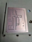
So here's my latest experiment, milling out a pcb on my CNC machine.

This is my best attempt so far, but I still need to work a bit on some auto leveling code. You can see how the traces in the lower right of middle did not get cut all the way through.

But, getting close. I can probably also condense this design down a bit.

Also need to get some better bits, but I'm not unhappy with how this is turning out so far...
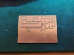
pcb_milled.jpg
 
Second attempt. I made a little waste block I attached to my spoil board with nylon bolts, then ran a flattening pass on that.
Yester day I used a .2mm 30 degree vbit, today a .1mm 60 degree vbit. So this one had a narrower taller v. I think I went a little too deep though which made the pads a little too small. Might be a little tough to solder on to them, but we'll see. I might actually give this one a shot and see how the soldering goes. My major concern is creating solder bridges that would cut across the isolation cuts.

So, 2 more things I'm planning on working on
1) I'm still researching how to do autoleveling with my firmware. I'm not sure if this version of the software has it in it or not. I remember when I put this control board in my machine I had to spend a good deal of time configuring and compiling the firmware. I did that on a virtual linux machine somewhere, and I can't seem to find it as I replaced my computer since then. Time to dig out some back up drives and look for it. Otherwise It's time to do some more research, lol

2) Solder mask. I've got some liquid solder mask that cures by uv light. You basically paint the circuit board with it. Take a printed image of just the pads on a transparency and place over the paint. The black dots on the transparency keep the paint from curing in those spots. Expose with a UV light, then peal off the transparency and clean off the pads. That's the theory anyway.

pcb_milled2.jpg
 
look a lot easier then back in the day. We used to do the circuit design using tape on mylar. Then we would apply a photo resist mask to the copper board and using a light table we would expose the copper coated board with the photo resist mylar on it to a strong light source. The we would use acid and it would strip away the copper from the board everywhere the light shined on the boar leaving the traces. It was a timely and messy process and we didn't have cad to do the design work.
 
I've been using a similar process to what you describe that works pretty well for me.
Basically, Clean the copper board really well, spray paint it with some flat black spray paint.
Then I use the laser to burn the paint off where I don't want the copper.
Then use the acid to etch it off. Actually works pretty good.
The only problem is that then I have to drill the holes by hand.
This process I can do one tool change and get the board milled an holes drilled.
 
Top